Over the past couple of years, I've had a couple of projects where I've designed and ordered PCBs. It's a great way to make more permanent electronics projects look and feel a lot less janky.
I've also come across a couple of open-source electronics projects where I had ordered PCBs from a project. For example, these drone timers (which I unfortunately am still yet to finish), and this drone controller screen adapter. It's super easy to download the design files from the project and upload them to a site and get them ordered - it's often a lot cheaper than finding them sold anywhere online (if they are at all).
I've also adventured into designing my own like a tiny DIY keyboard based on the ARTSEY.io layout.
For this post, I'll go over the basic principles I've learned for creating a PCB from scratch - from design, all the way to ordering. I like to use KiCad which is free and open-source, but there's lots of other great PCB design programs, both free and paid, even ones that work in your web browser. As far as I know, they all work pretty similarly, so these basics should transfer across.
The project I'll make here, is going to be a with a microcontroller, button and LED.
Building a schematic
First up, we need to build the circuit's schematic, this is a high-level overview of components and how they connect.
I'd actually usually start with a breadboard design before doing this, just to check it works in the real-world first, but you could also do this part after designing the schematic. It all depends how you like to work.
To get started, launch KiCad and create a new project. I've called mine simple here. You'll see it's automatically created files for the schematic (simple.kicad_sch), as well as the PCB (simple.kicad_pcb).
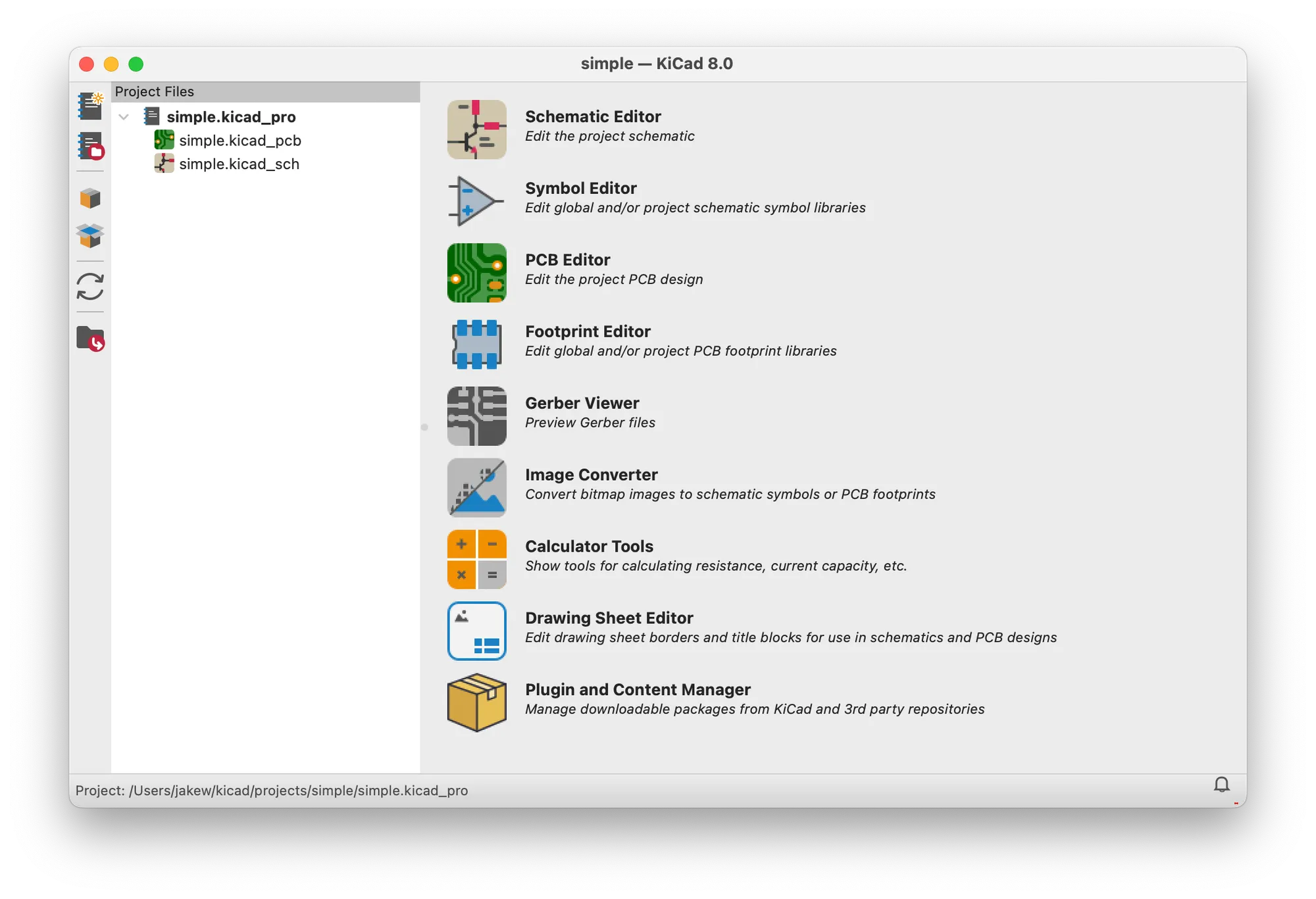
This post is just going to touch on the Schematic Editor and PCB Editor, but I'll give a super quick explanation for a couple of the other options:
- Symbol Editor - this is for editing symbols or components for use in the Schematic Editor. There's lots of built-in parts, but if a part you want isn't in there, you can use this to import it from someone else who has designed the part online, or create your own part from scratch.
- Footprint Editor - the same as above but for the PCB Editor instead. These footprints will likely be linked to symbols in the Symbol Editor.
- Gerber Viewer - Gerbers are the exported design files that we'll eventually send off when ordering. You can view them using this tool.
- Plugin and Content Manager - this lets you add extra components and plugins. For example, when I was designing my keyboard, I was able to find a component library for keyboard switches in here.
If you open up the Schematic Editor, you'll see a blank page with a lot of buttons around the outside.
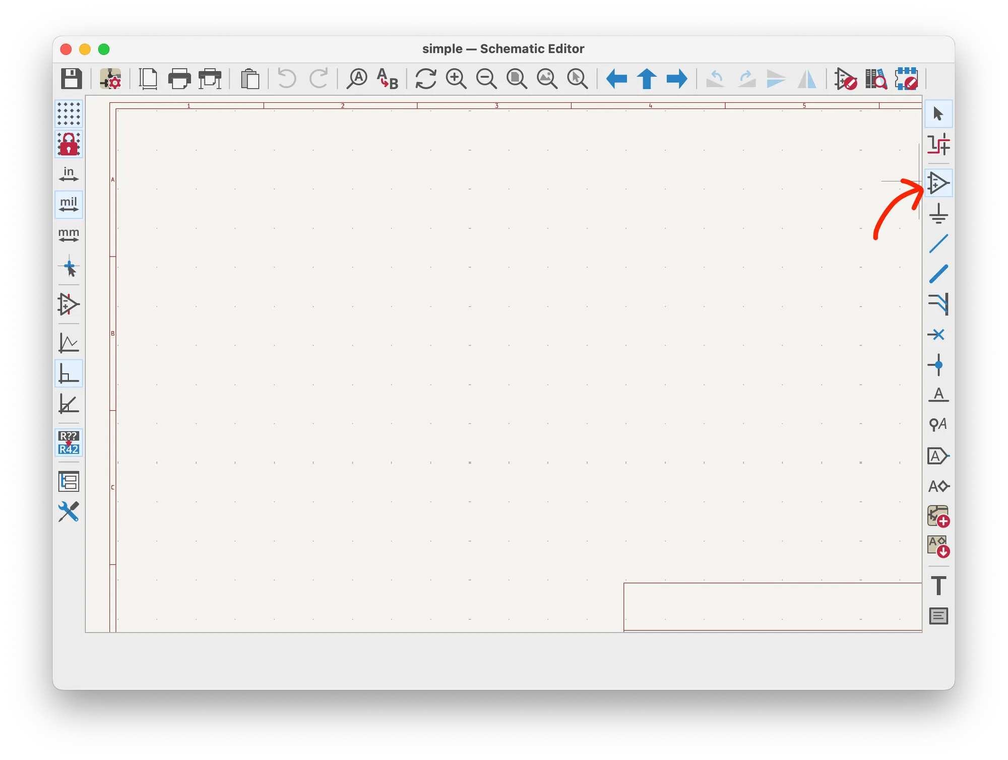
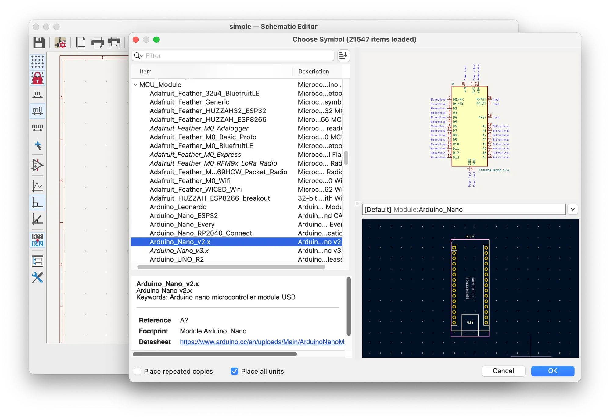
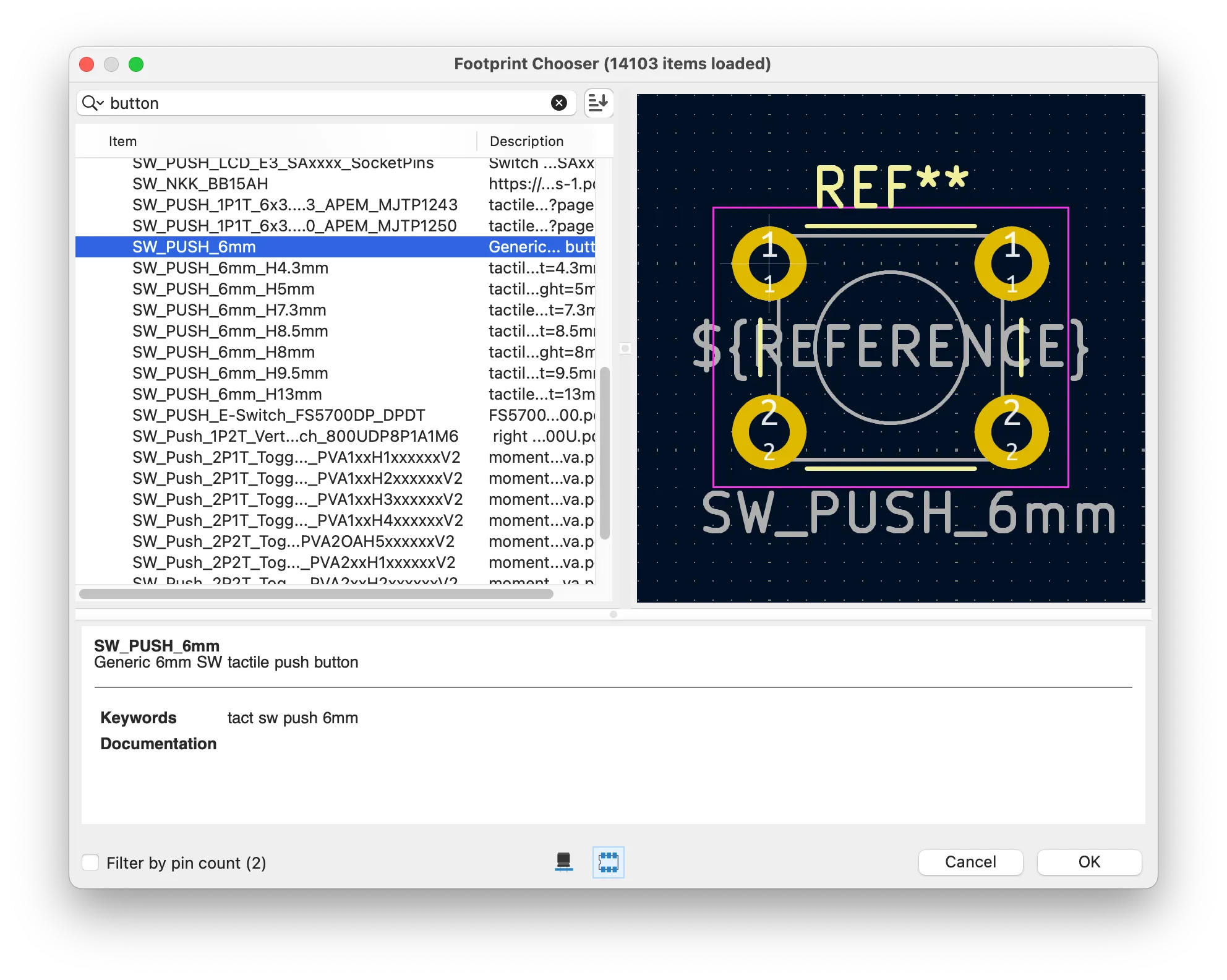
First off we need to add components to the schematic. Use the 'Add Symbols' button on the right toolbar, which will bring up this window to select a symbol. A symbol is just a component in the schematic. For simplicity, I'll use a built-in one here, an Arduino Nano. The top right of the window shows the symbol as it will appear in the schematic, and the bottom right shows the footprint, which is as it will appear on the PCB. The dropdown in between the two previews lets you select a flavour of the footprint. For this Arduino Nano, there's just with mounting holes or without, but for more complicated components, you might need to select the size of component you're planning to use (e.g. size of a surface mount resistor or type of switch) - essentially make sure the footprint matches the real component you want to use.
After you press OK, click anywhere on the schematic to place the symbol. Now I'll add in a battery, button, LED and a resistor for the LED. The battery and button didn't have footprints for me, so I've left them blank and we'll sort them later. Here's where we're at:
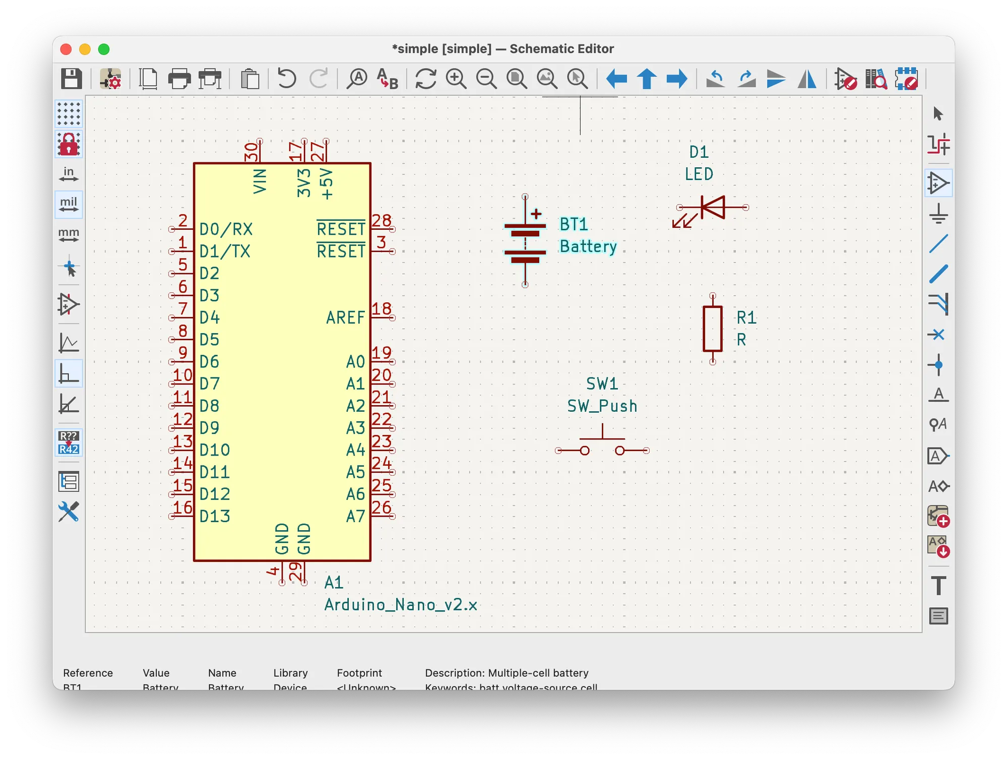
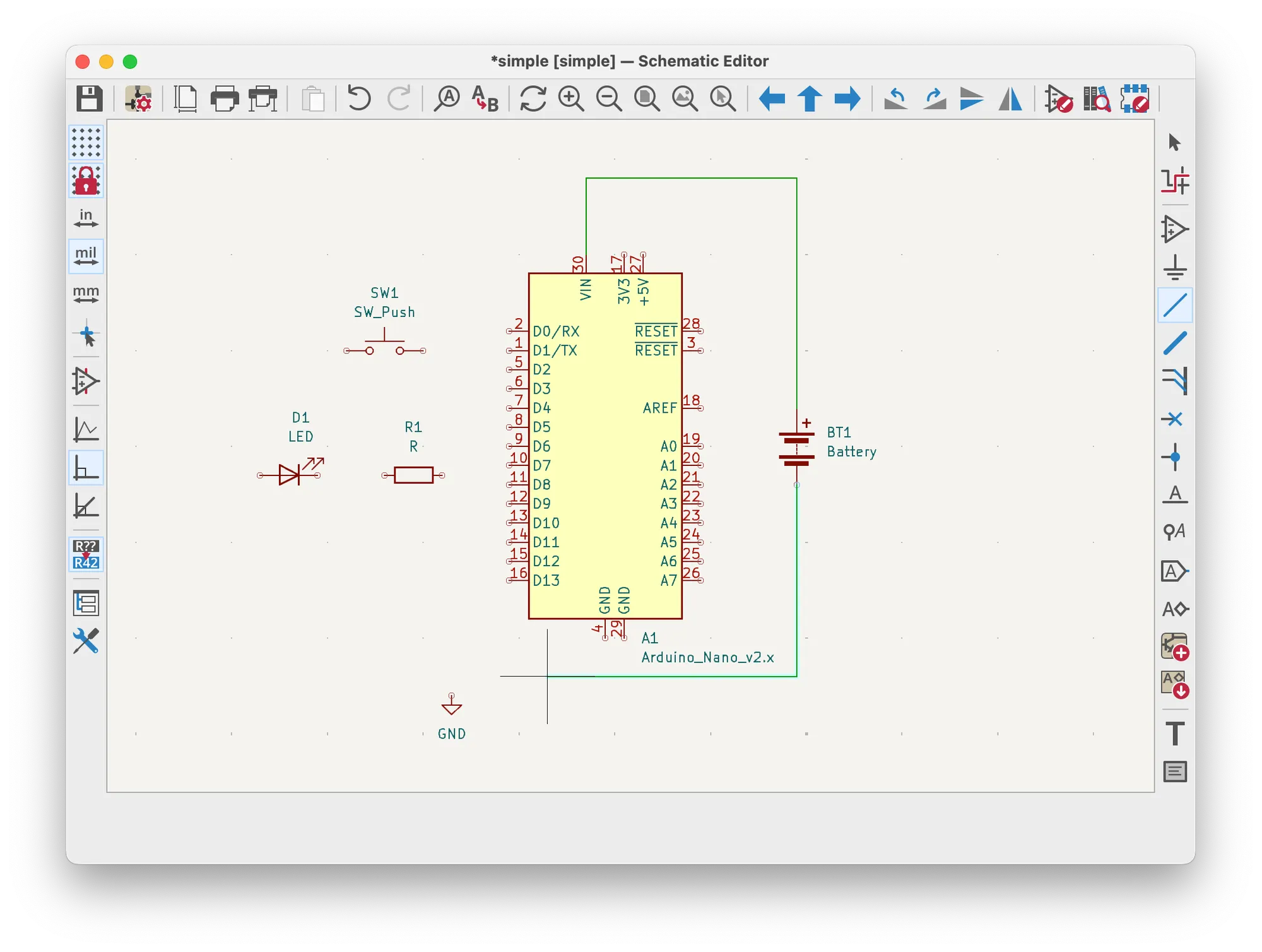
I've moved all the components around so they are laid out better, then finally we'll add in a ground connection using the symbol underneath the one we just added. You could also add in a +5v connection if you wanted. I'm not sure if this is strictly necessary, but it makes the diagram slightly clearer and it may help out later on when we're putting a ground plane on our PCB (but more on that later...)
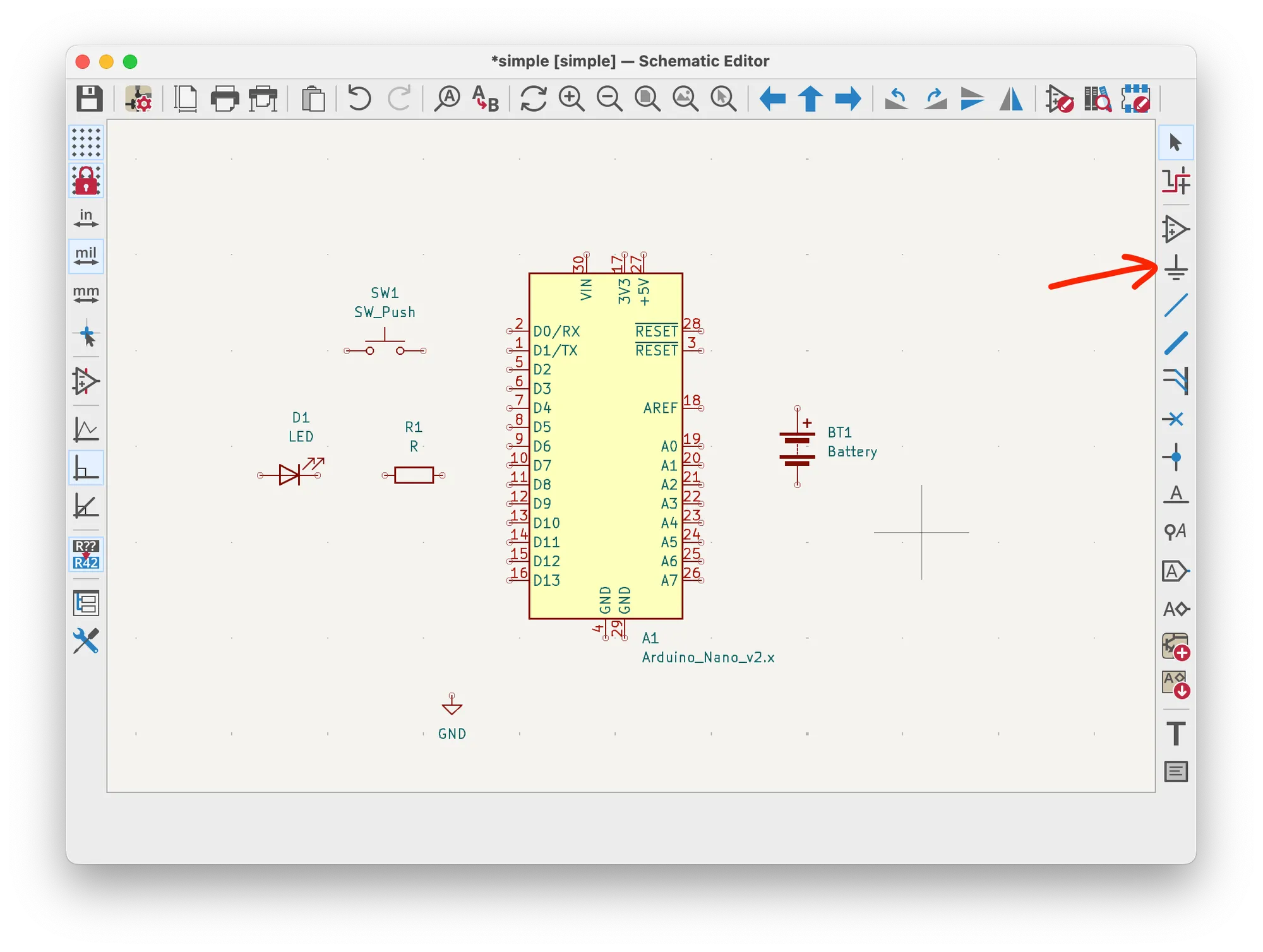
Now use the next icon down on the right to create some wires to connect all the components. Just click on one of the circles at the connection points on a component, then click one of the circles on another component.
Here's my final schematic:
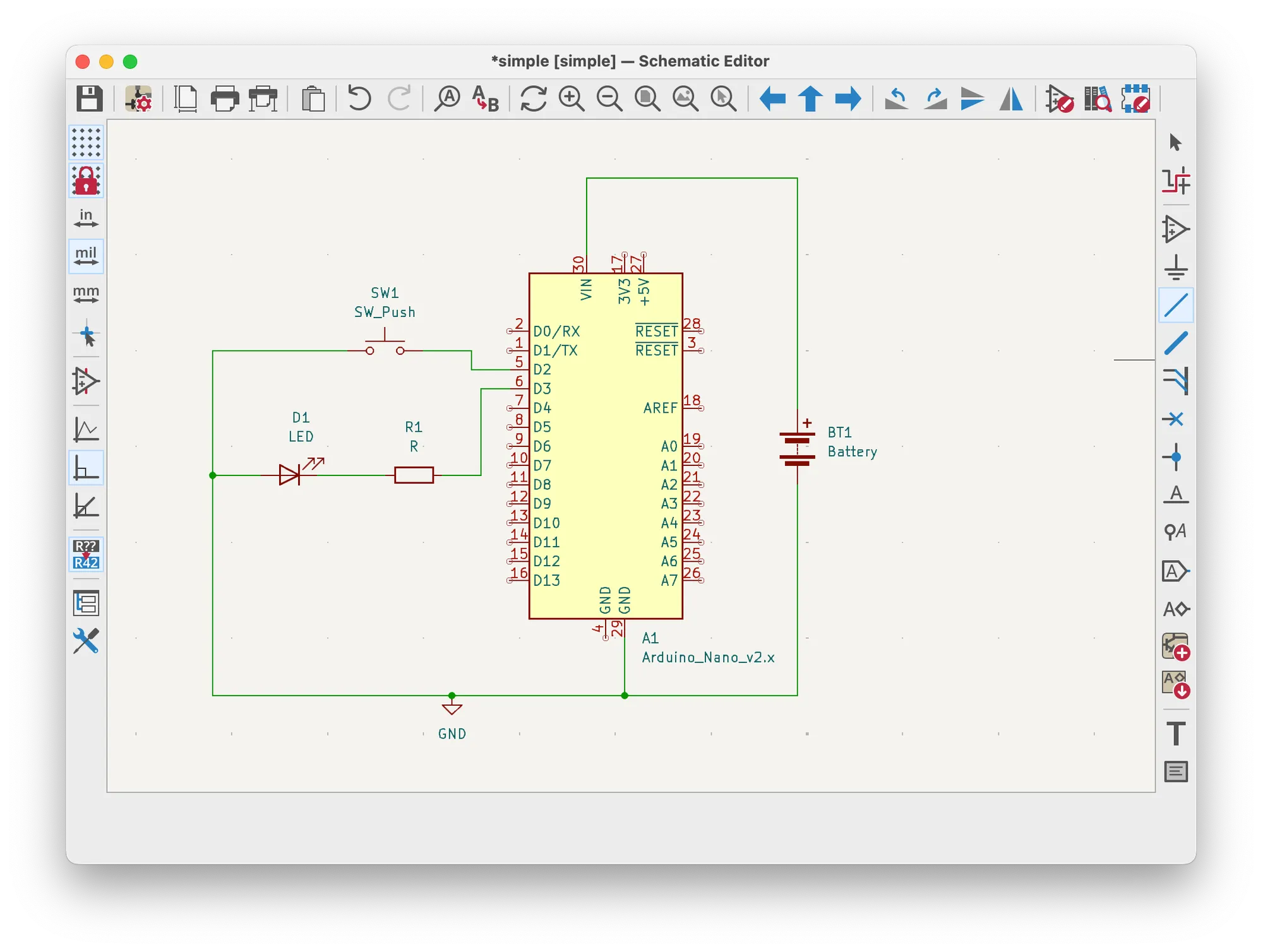
That's pretty much all we need to do for the schematic, now just save it. You can also add labels to your diagram, using the label and global net label tools near the bottom on the right which can give your connections nicer names. There's not much going on here, but for more complex schematics it can help a lot with laying out things. It lets you have connections between multiple places on the schematic without drawing wires everywhere, just connect a global net label at each end.
Designing the PCB
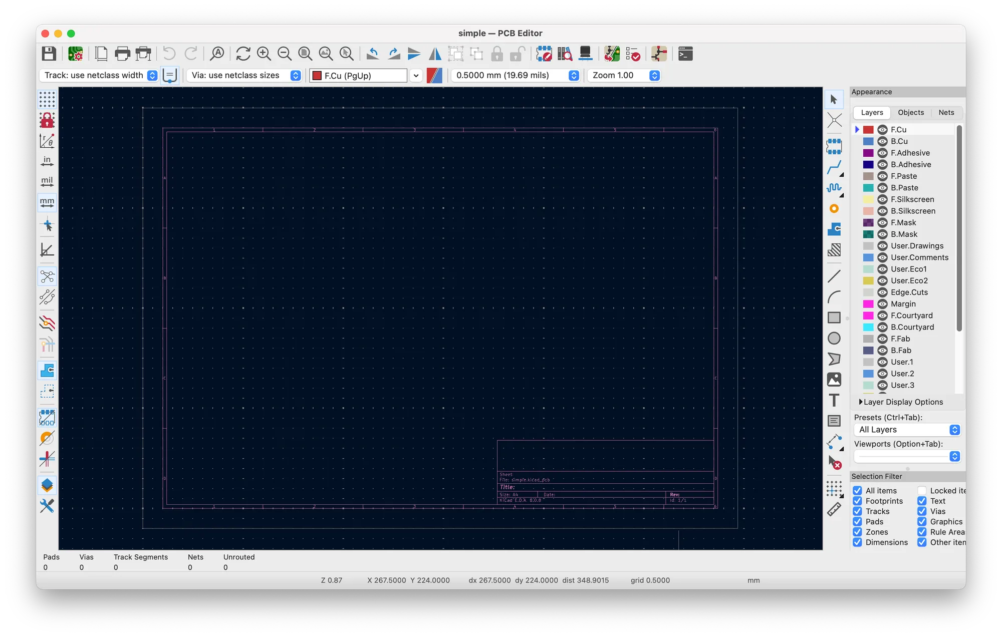
So now we've got the schematic designed, we can move onto the PCB. Head back to the KiCad project window and open the PCB editor. This window also has a lot of buttons and things.
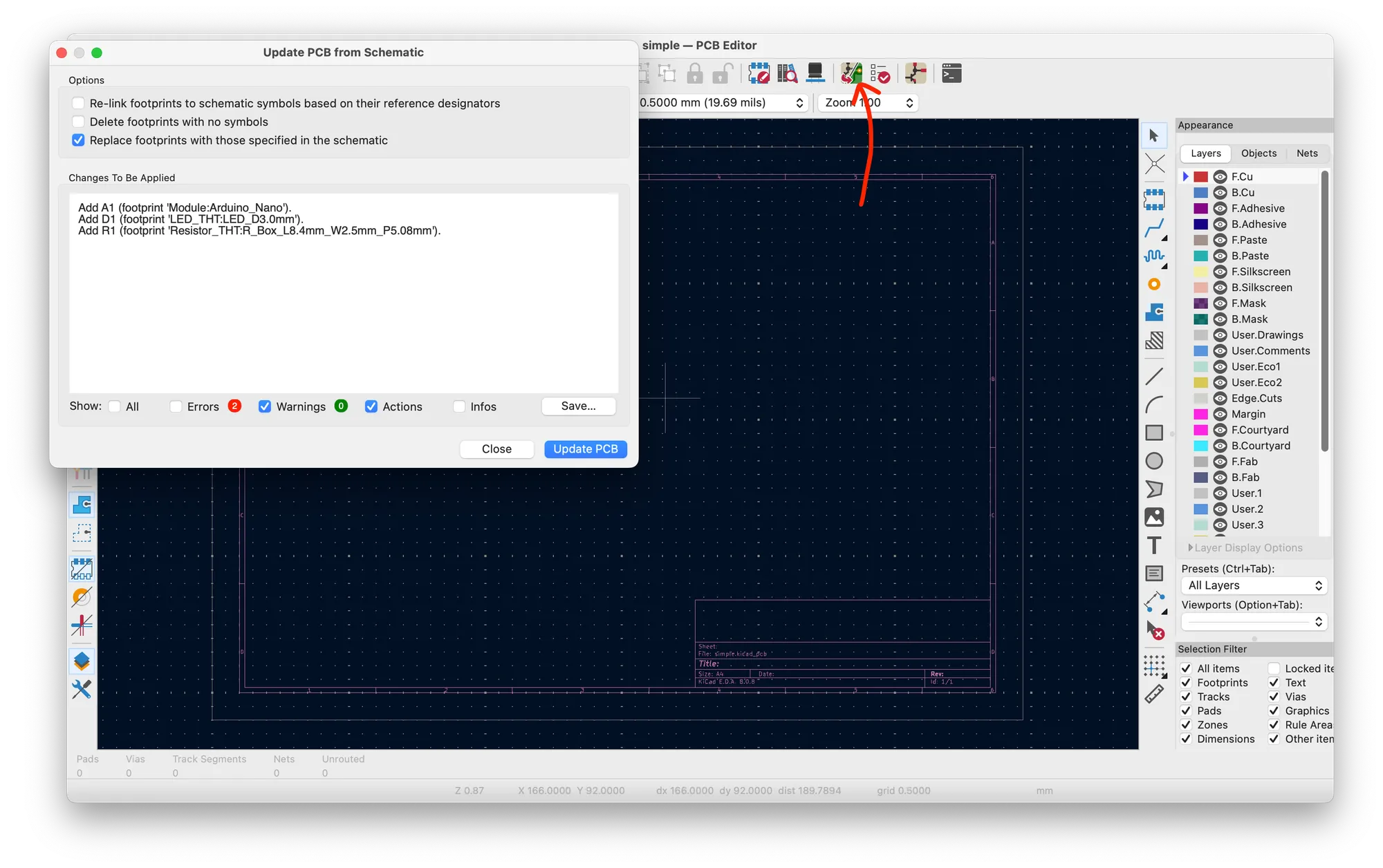
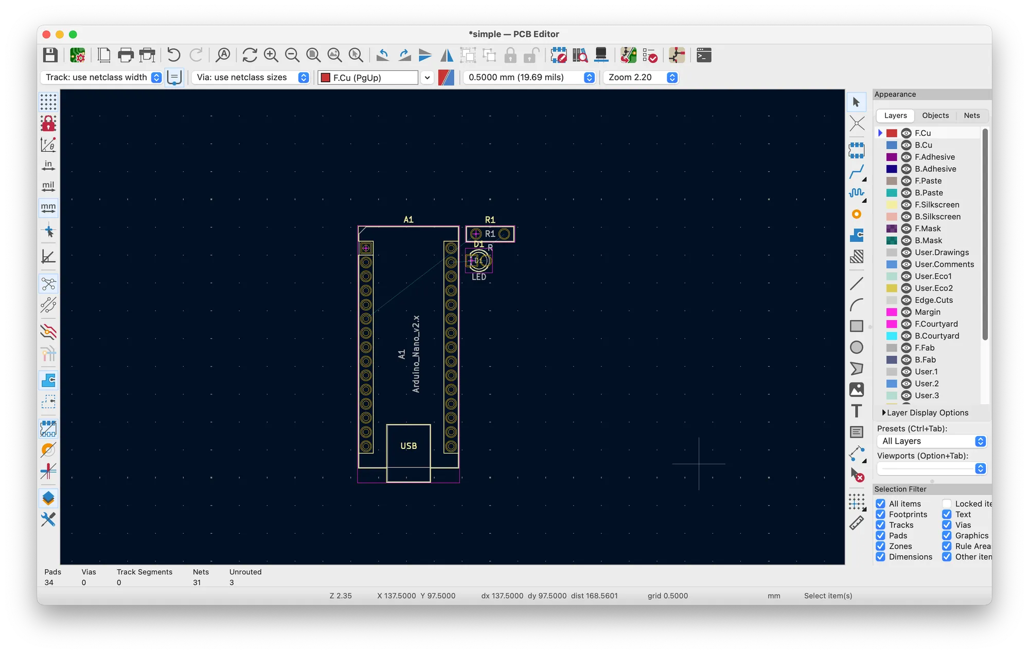
We can use this button at the top to import the components from the schematic. It'll give you a quick summary of what it's going to change (as you can also go back to the schematic and add more things later, then do this again to update the changes that have been made). Once done, you'll see the footprints added to the PCB.
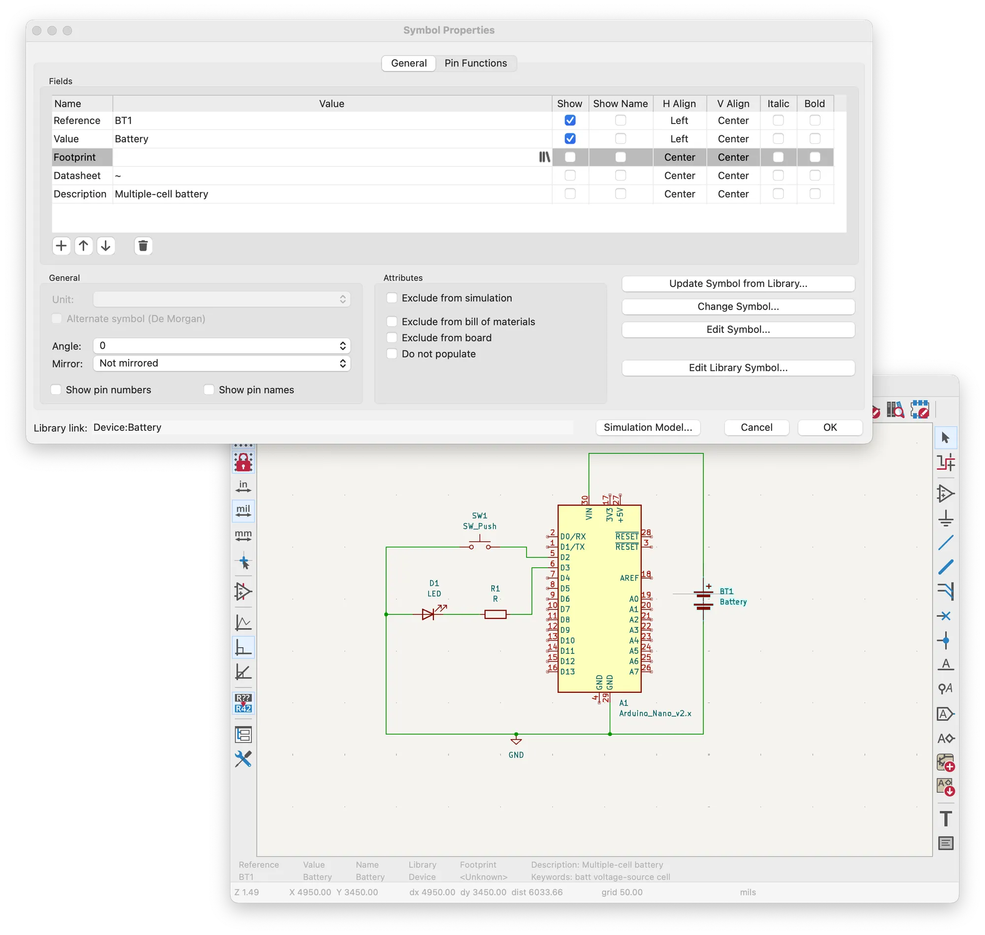
For the few components that aren't shown, we can go back to the schematic editor and change the footprint to be used by double clicking on the symbol, then change the footprint by clicking the lines in the value box to bring up the footprint selector.
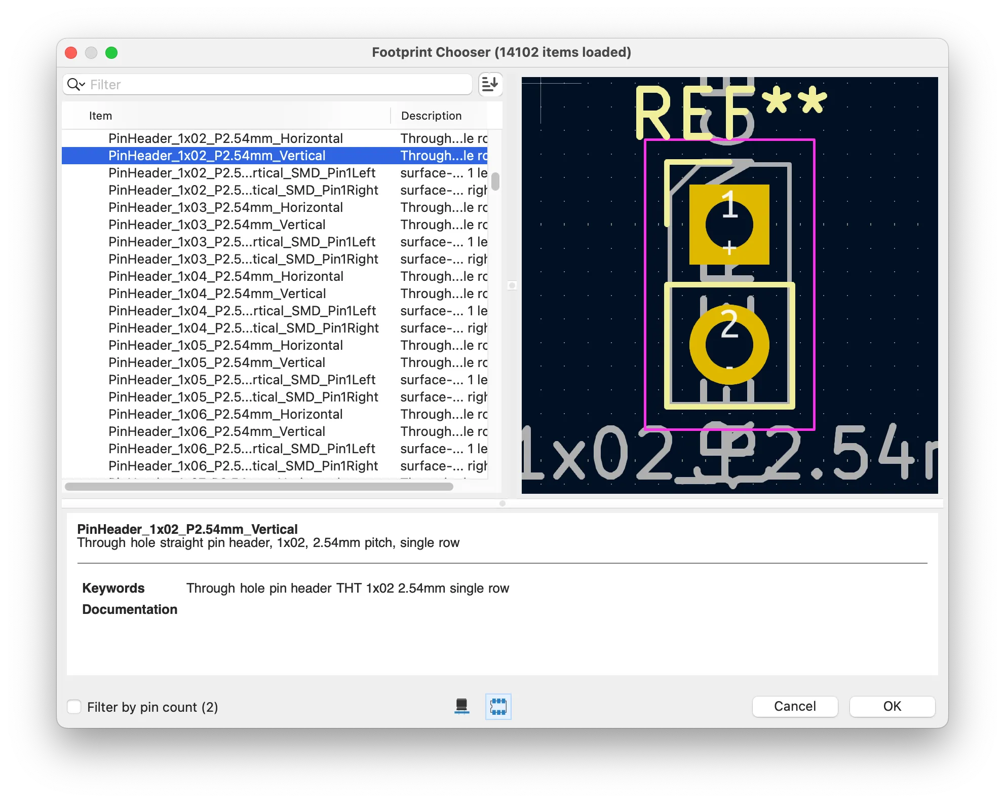
For anything missing, you might need to find something close, or find footprints others have designed online, or create your own. For the battery, I'll select a 2-pin header which will allow the circuit to be powered from an external 5v supply. Strangely, there is push button footprints available, they just weren't linked to the symbol earlier for some reason.
After making these symbol changes, redo the previous step again to import the new footprints. You'll notice some thin blue lines going between the components. This is how they should be connected together according to the schematic.
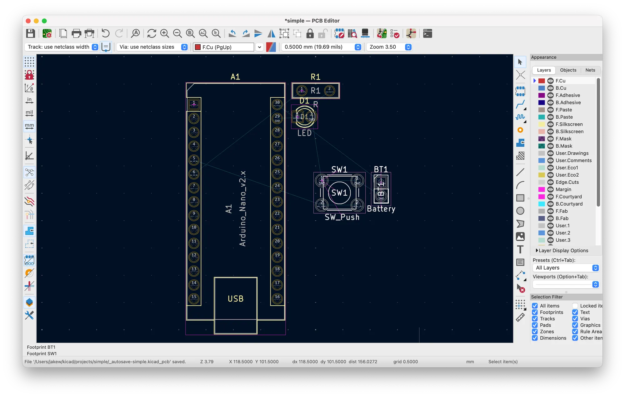
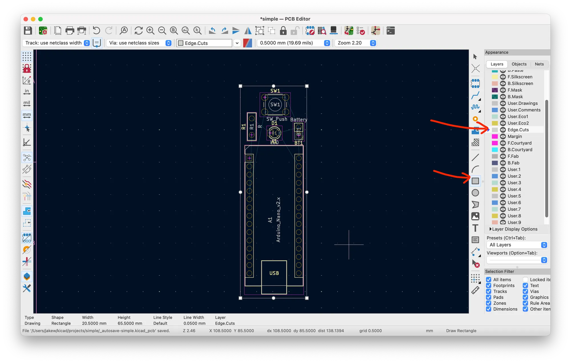
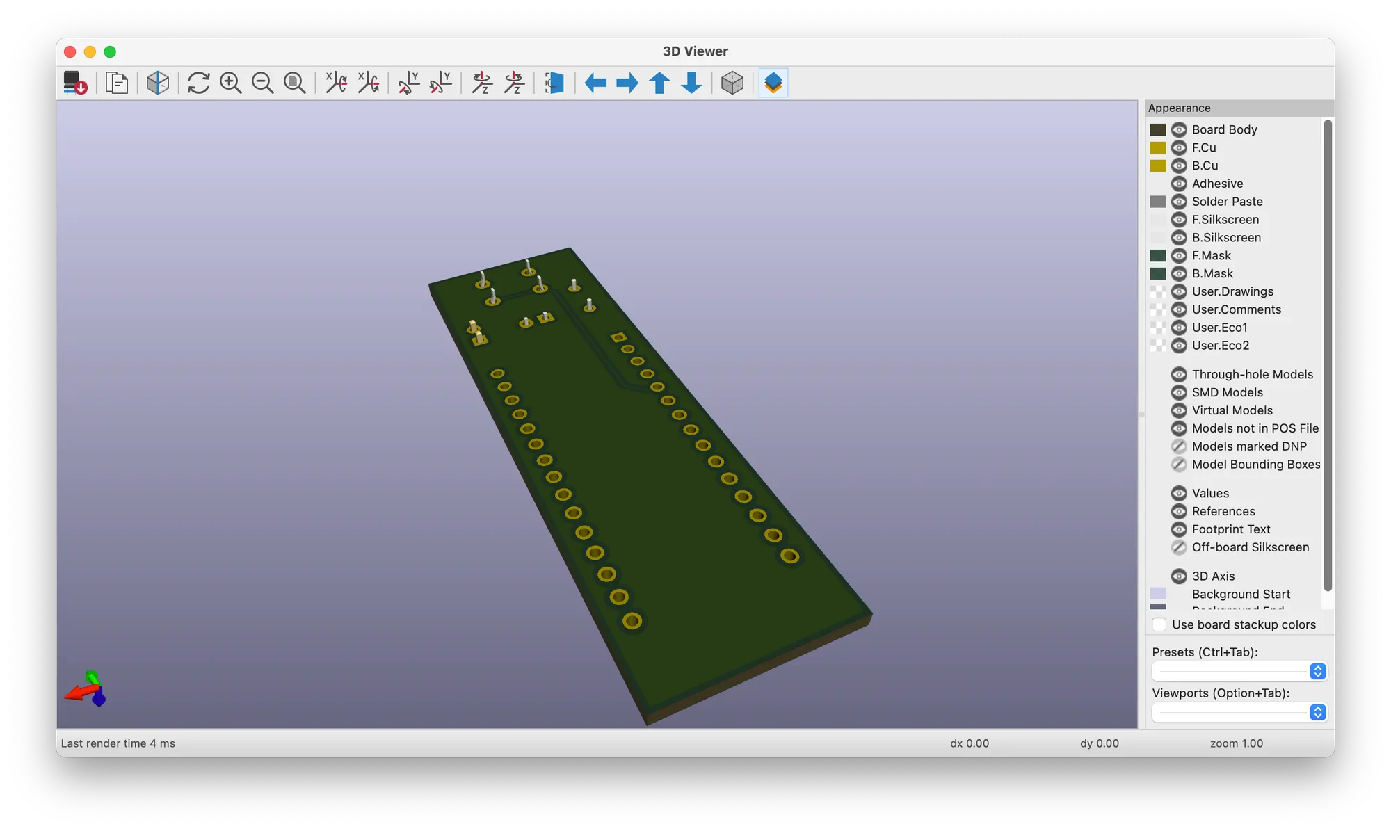
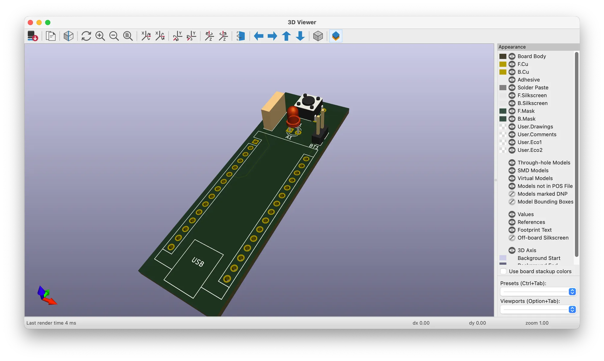
Now I would lay out the components to near the pins they are going to connect to. Once you're happy with the layout, click on the Edge.Cuts layer on the right side. As the name suggests, this is cuts that the manufacturer will make, so we want to put one around the edge of the board. If you're feeling extra fancy, you could add in rounded corners, mounting holes or other things. You might notice some of the components, for example, the LED already have holes where the legs go through the board.
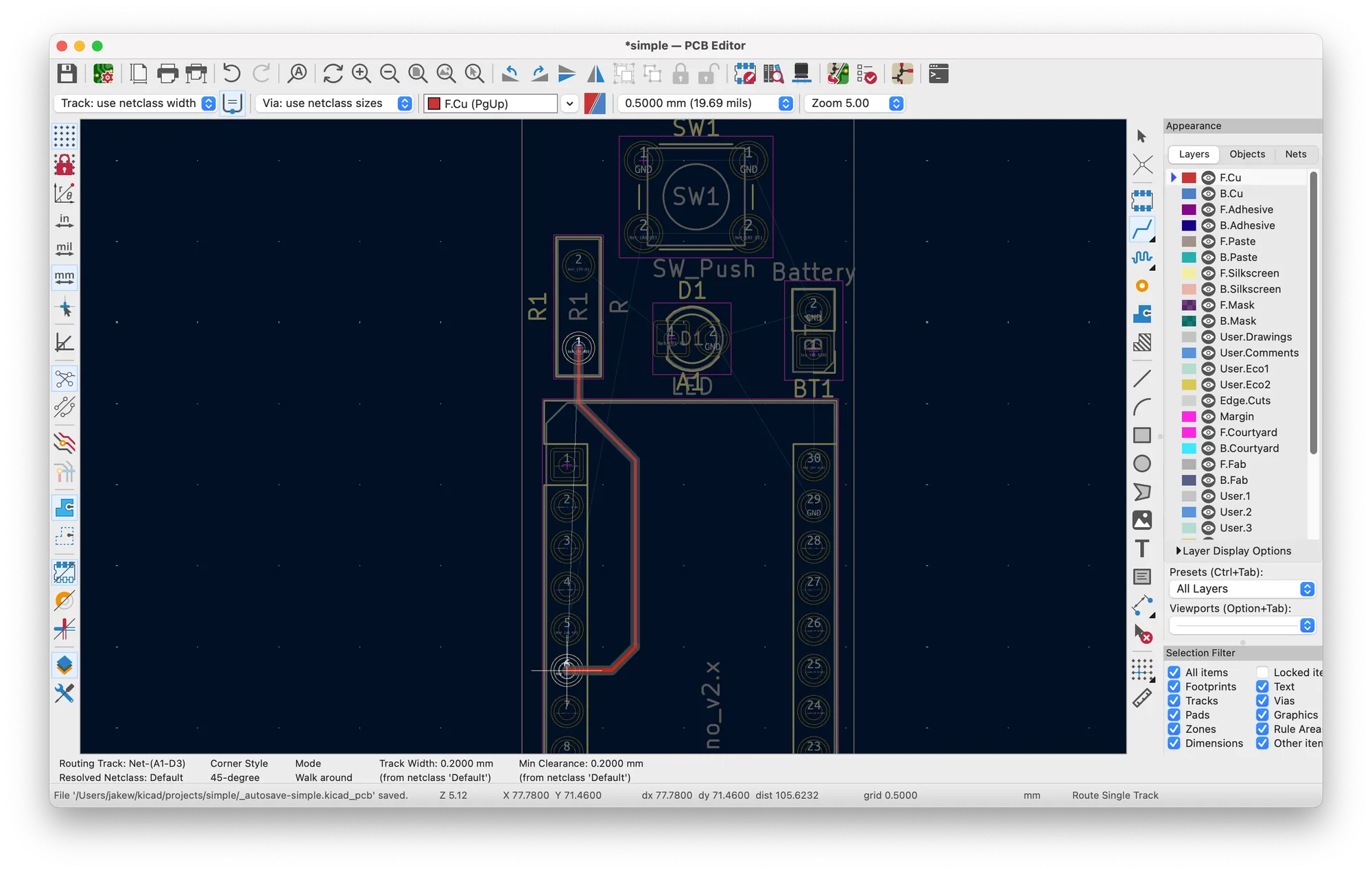
Some of the layers have F & B prefixes, which means front and back. We'll use the F.Cu (front copper) and B.Cu (back copper) for traces between components and you can add printed text or images to the board using F.Silkscreen and B.Silkscreen (although remember to reverse text if using the back). Click on one of the copper layers then use the first blue line on the right toolbar to create a trace. You'll notice it'll helpfully highlight where it needs to go. Make sure to leave the ground connections for now, because we're going to make a ground plane to connect them all. Here I've used the back copper layer to run a trace along the back of the board because I've got two tracks that overlap. With more complex PCBs it can be a bit tricky to route everything around, but it's all part of the fun!
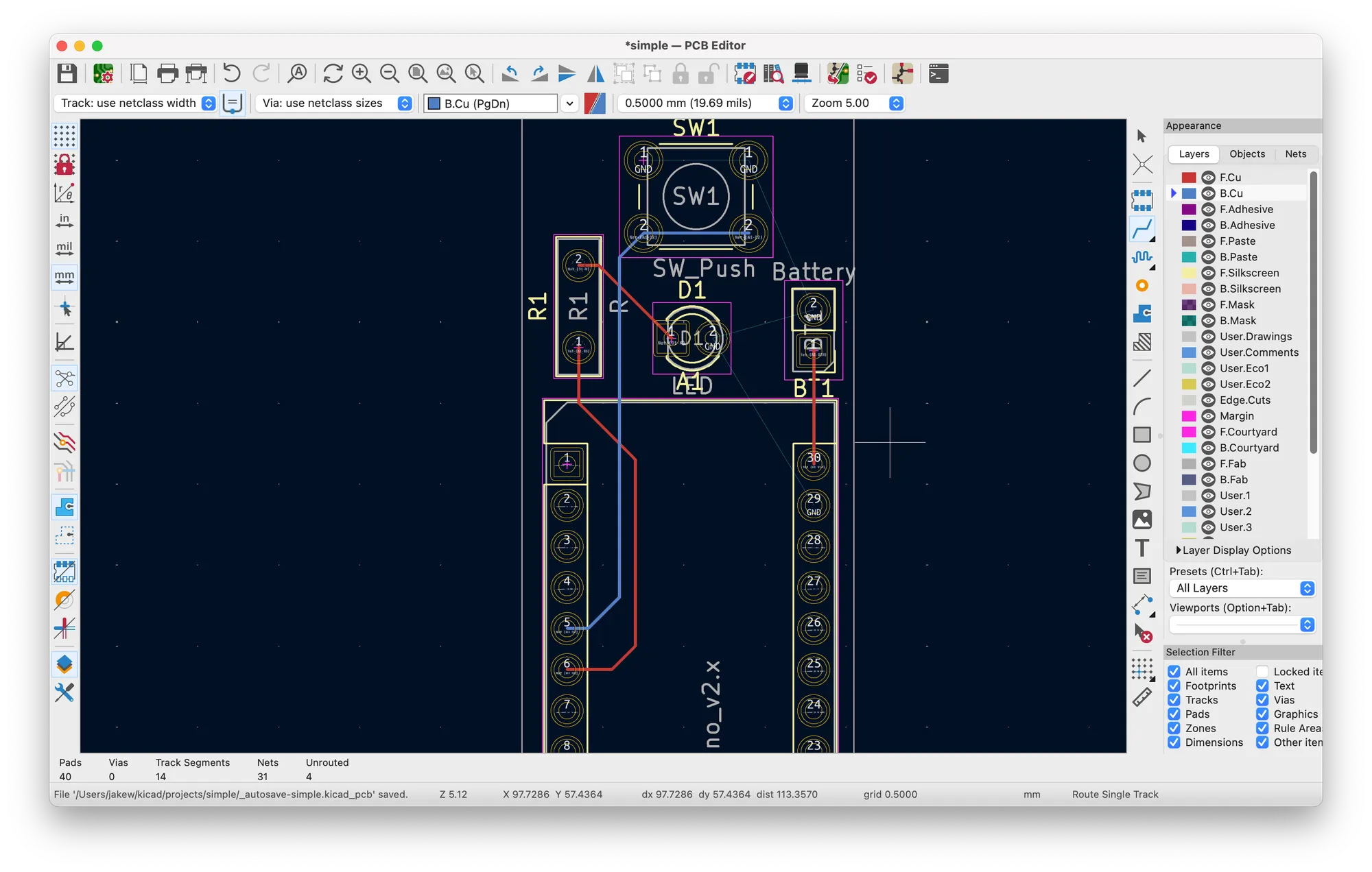
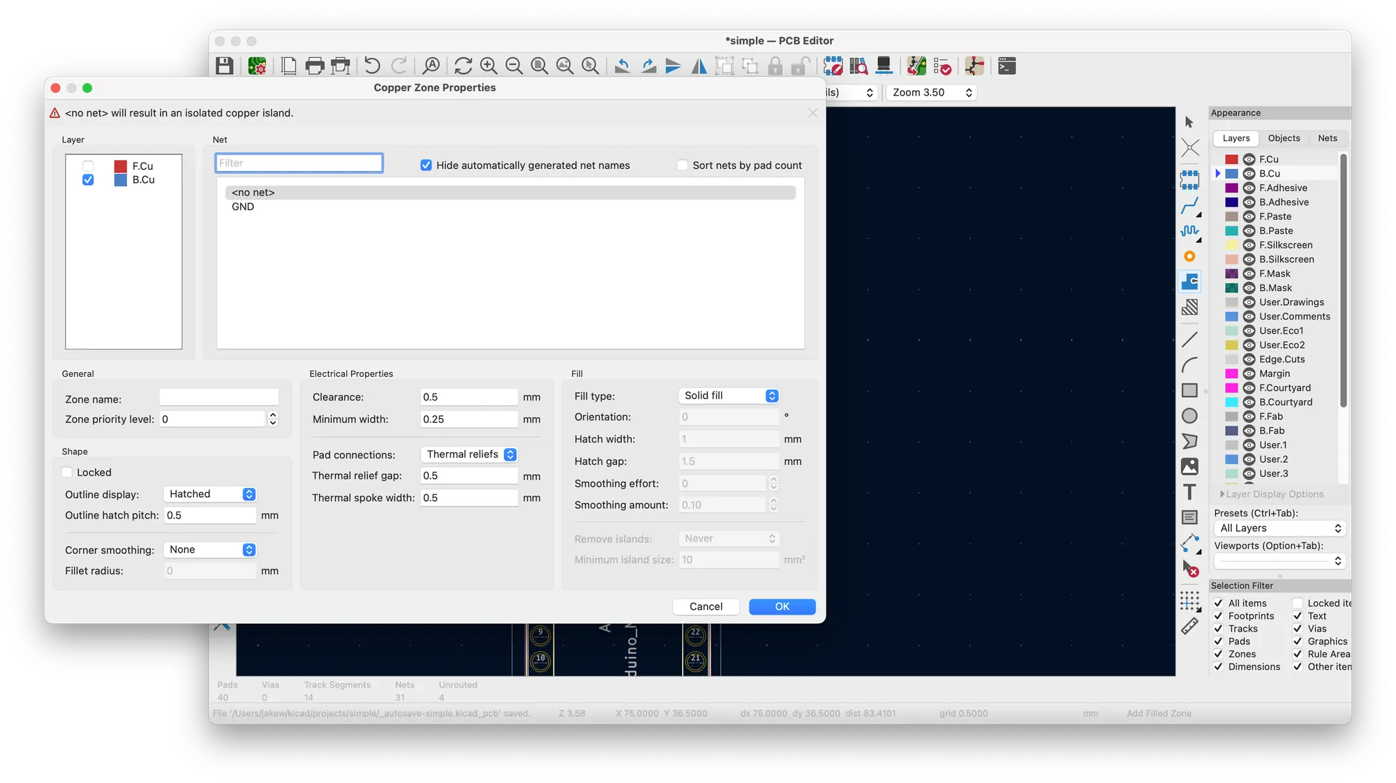
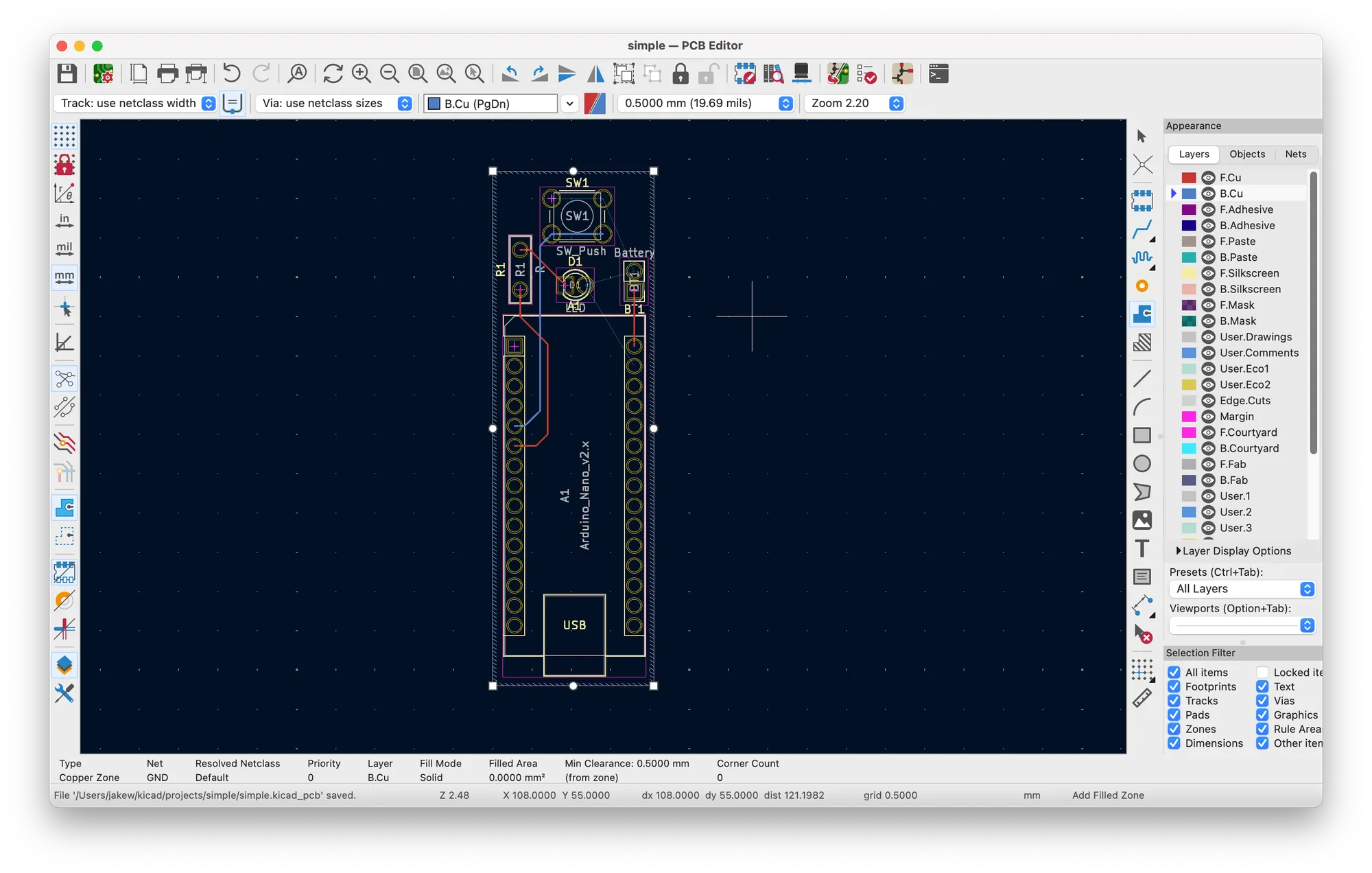
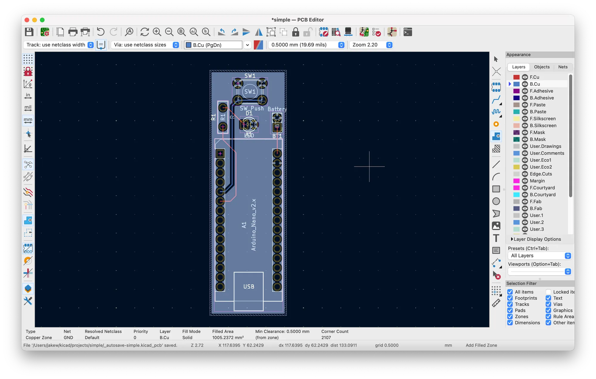
Now we'll use the copper zone tool which is the blue shape on the right that has a wire going into it. This creates a zone of copper on the board. We should add a ground zone on the board when we're done. This can help with any external interference on the circuit. Select either one of the copper layers in the window that appears, then select the GND net and draw a box around the board again. Finally, go to "Edit" then "Fill All Zones". You'll see the board now has copper everywhere, except where we've got the blue trace going through. And it connects up the ground pins on the components that need it.
Now I like to go to the 3D viewer (icon left of our schematic import tool) and give the board a check to make sure it looks okay and all the traces are connected up where they need to go.
There's also an automated checking tool named DRC which can help spot any issues with your board which I'd recommend using before ordering. But, I'm happy with this board, so lets go and order it!
Ordering the design
Once your happy with your PCB design, it's time to get it ordered. You can find a bunch of manufacturers online and can easily find one to get boards created and shipped for under £10, albeit they take a little while.
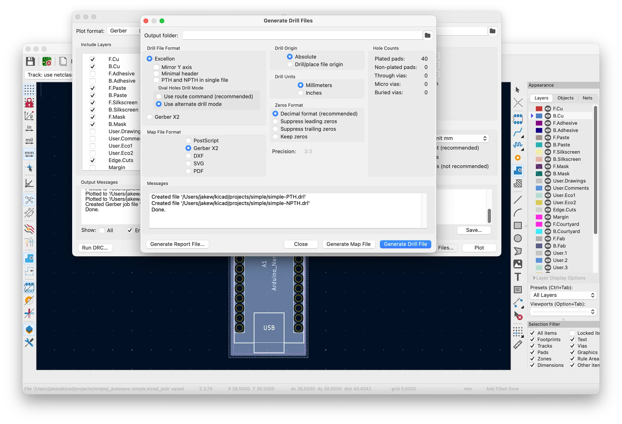
Regardless of where you choose to order, we need to export the PCB to gerber files. This is what the manufacturer uses to make your PCB. In the PCB editor, go to "File", then "Fabrication Outputs", then "Gerbers (.gbr)". The settings in here depend on your manufacturer so make sure to check their website for suggested settings. Once dialed in, click "Plot" to export, then "Generate Drill Files..." and do the same there. You should have a bunch of files generated now. If you choose to use PCBWay like me, they actually have a KiCad extension which allows you to upload your design to their site with one click, so there's no need to faff around with these Gerber settings.
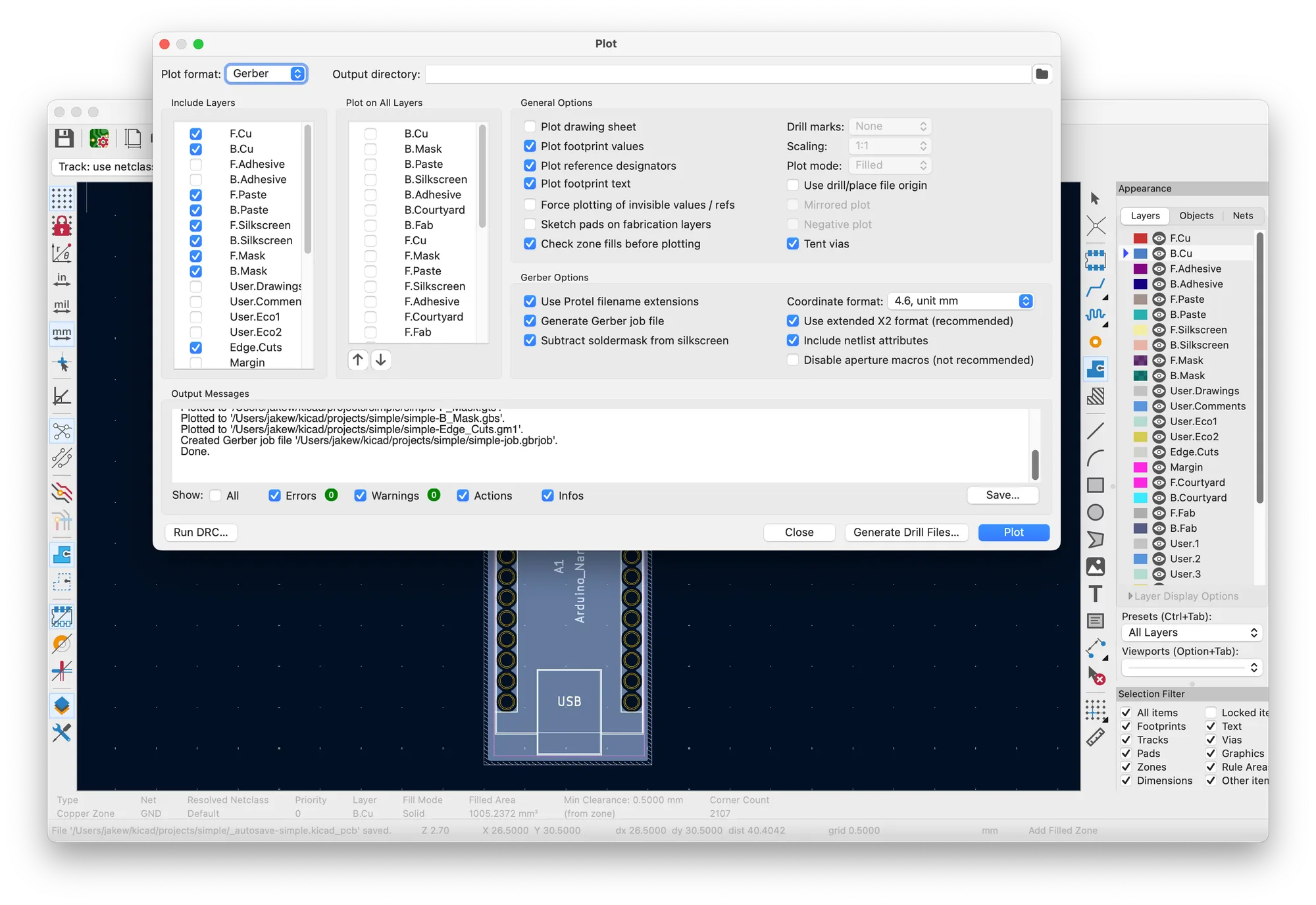
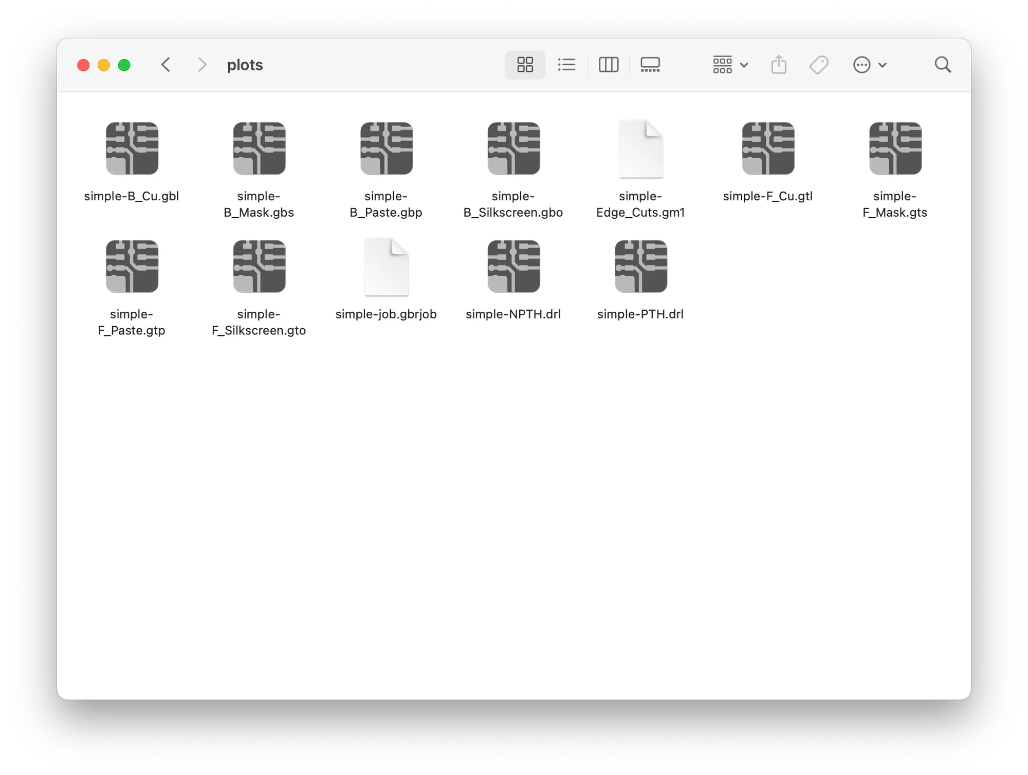
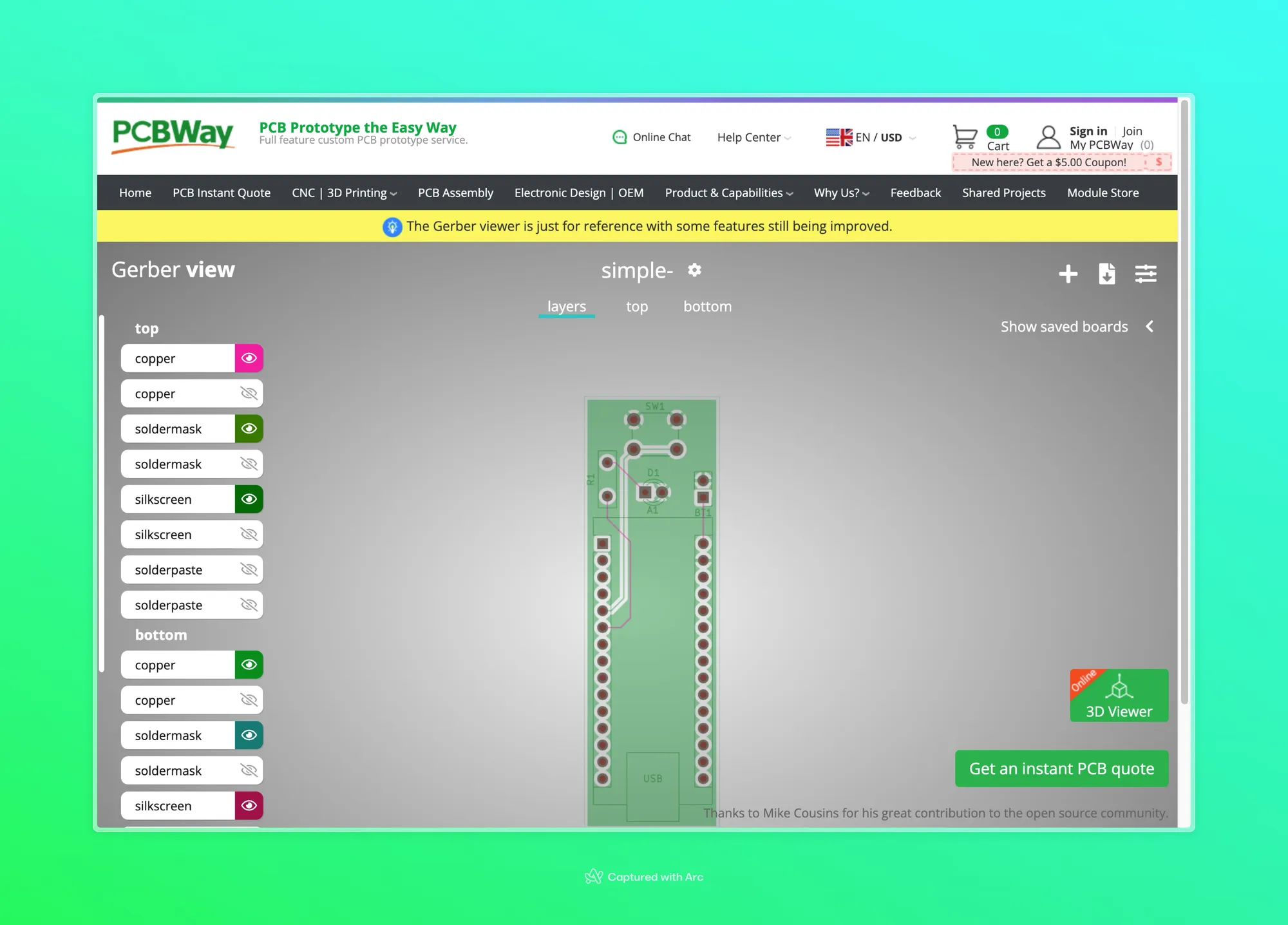
You'll want to ZIP up the Gerber files now. I like to then take it to a couple of online Gerber viewers to double check the design again. For example, this one from PCBWay. It's a good idea to check on multiple viewers to make sure there's not an issue that arises with just one of them.
Once I'm happy that the design looks fine, I'll upload the design to the manufacturer. PCBWay have kindly given me some credit towards my next project, so I'm going over the process of ordering with them. There's also many other choices for manufacturers, both local and abroad, basically it depends on how fast you want your design and the quality you'd like.
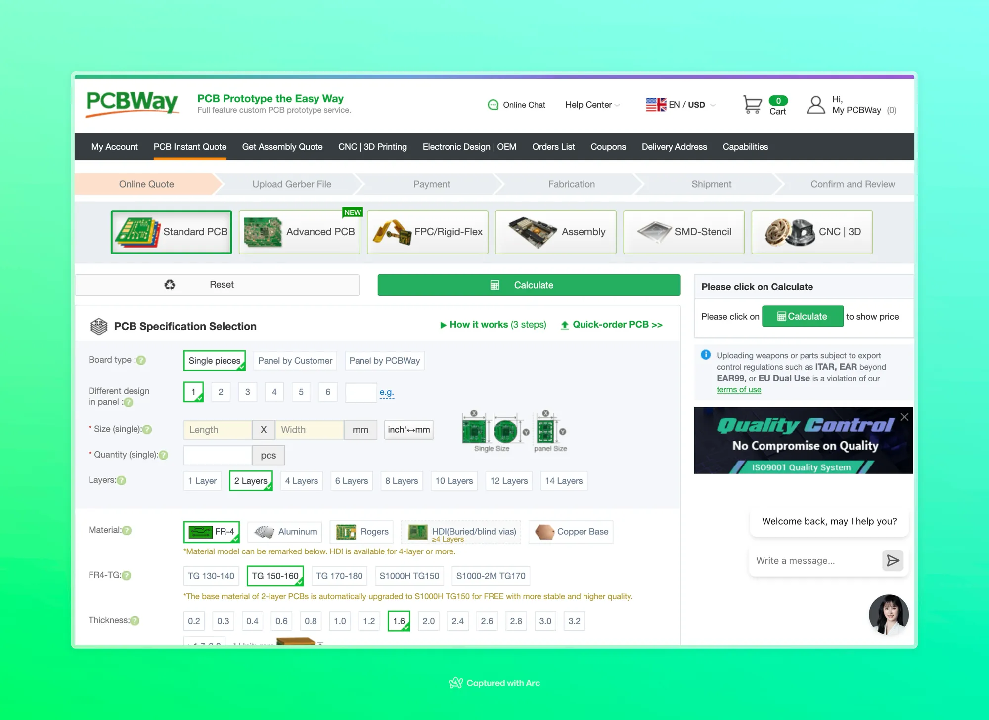
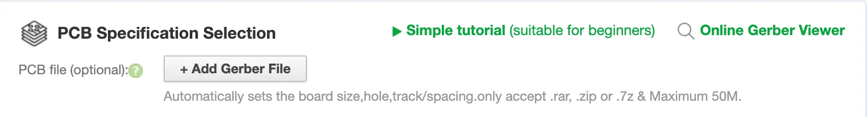
On PCBWay, when going to order the board, you can use the 'Quick-order PCB' button to upload your files straight away, which will automatically calculate the size and show a preview at the top of the page. Underneath we've got a bunch of options to select. There should be similar options for other manufacturers too.
So first thing we'll do is upload our zipped up Gerber files. You should see a preview of the board after uploading, and it's another good chance to double check your design looks as it should. The site should automatically calculate the size of the board.
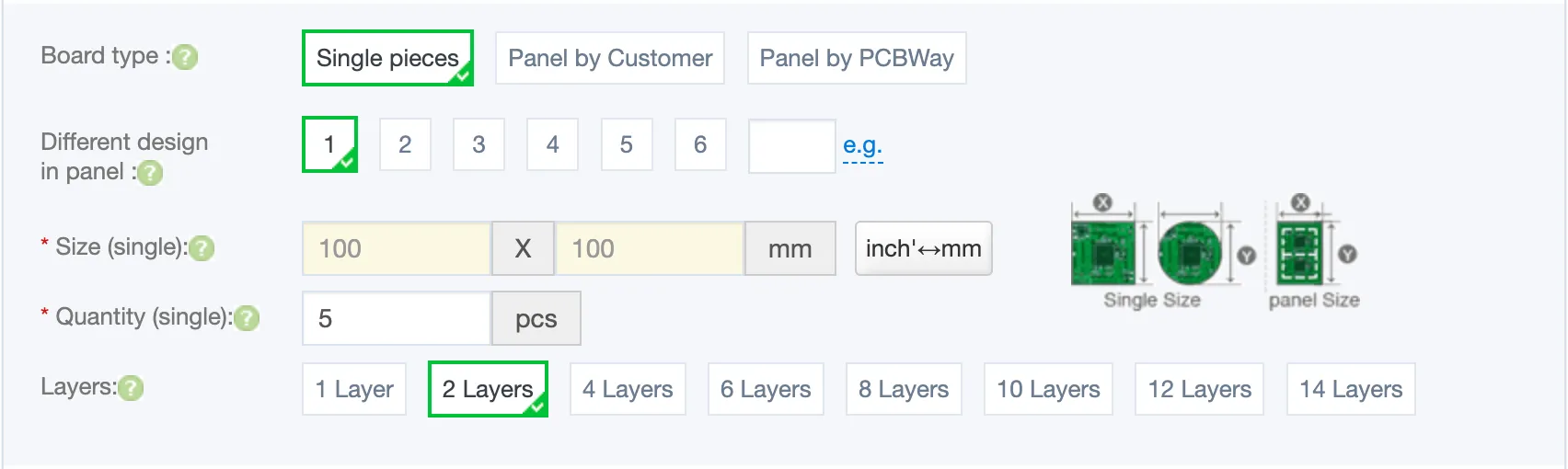
For the board type, there's a few choices. Unless you're doing lots of PCB assembly, you don't need a panel. You can see an example of a panel on the right of this screenshot, it's where boards come stuck together on a big board and you would separate them off after assembly.
For quantities, many manufacturers have a minimum order quantity of 5 boards. It might seem like a waste but it's always good to have a spare or two in case you mess up.
For layers, we're using 2, this is because we've got the front & back copper. You'll find anything higher will cost more money, but for most projects you should be able to get away with 2 layers. For more complex projects, you might want layers of copper sandwiched in the middle to give more space for routing.
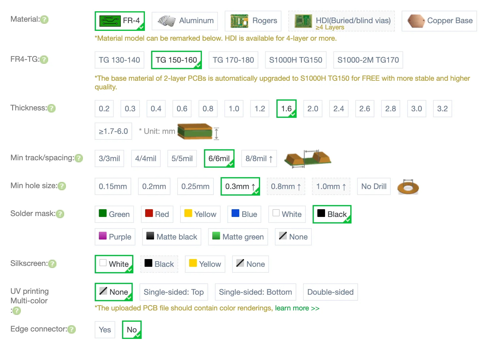
- For material, FR-4 is standard, with the others being used for special applications.
- For the FR4-TG, this is the kind of quality for the board, particularly the temperature threshold of the board. The pre-selected one should be okay for most use cases.
- For thickness, you might need to choose something else depending on your project. For example, if you're making a board that fits into a USB port it'll need to be 2mm. Otherwise, the normal 1.6mm thickness is great.
- For minimum track/spacing and hole size, you'll need to double check your design. You can set constraints in KiCad for this by going to File > Board Setup > Design Rules > Constraints, after setting you can run a DRC check to check the spacing of everything.
- For solder mask, you can choose whatever you like, this is the main colour of the board. Here I've gone for black, but strange colours can adjust the price of the board.
- For silkscreen, again, you can choose whatever, but it may affect the price.
- UV printing allows multi-colour prints on a board. I'm not going to cover that here, but it's a feature PCBWay has that I've not noticed at any other manufacturer.
- For edge connector, this is if you have connection points on the edge of the board. Think like how a graphics card has the gold plated connector on the bottom edge of the board. Again, you'll only need to select this for specific applications.
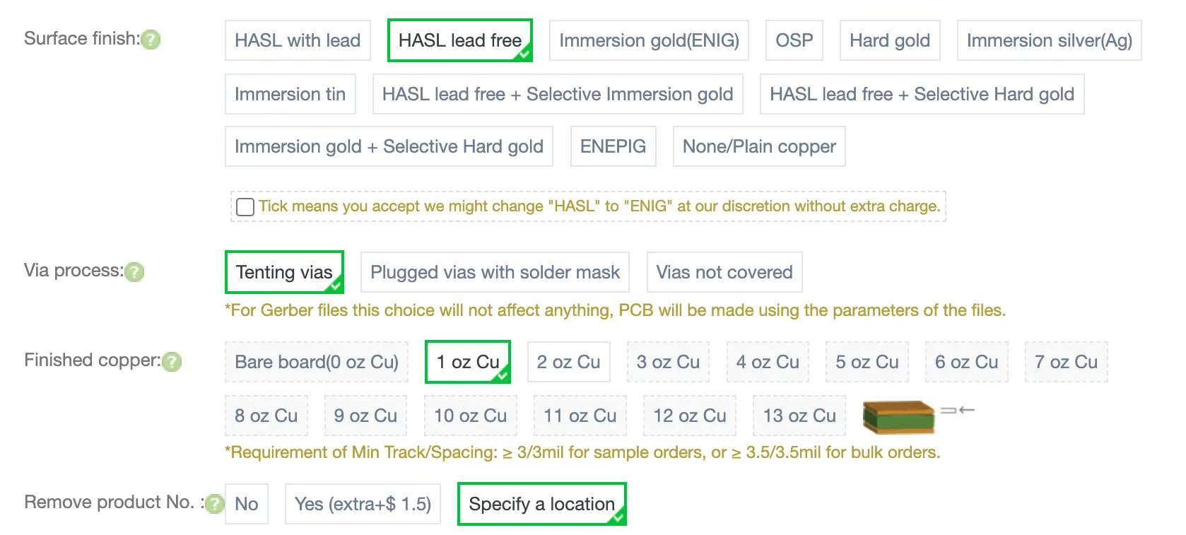
- For surface finish, there's a bunch of options. For the most part, HASL lead, and HASL lead free are the two standard ones. I like to choose lead free just so I feel a little better about all the solder fumes when assembling my board later on! ENIG offers a stronger finish while costing a little extra, and may of the others you probably won't need for normal use cases.
- For via process, tenting vias is the standard, but as you can see this option for PCBWay is dictated by the Gerber files, so no need to make any changes to this. KiCad uses tented vias by default.
- For finished copper, this is how much copper that is used on the outer sides of the board. A higher number is stronger, but for most cases, 1oz is fine.
- At PCBWay, and other manufacturers, you can chose to remove or specify a location for the product number. This is just a code that identifies your order. Removing it completely costs a little extra, but you can move it to anywhere you like for free. I like to put it in one of the back corners of the board. Make sure you check with your manufacturer about how to specify the location. For example, for PCBWay I need to add the text 'WayWayWay' to my board.
Now you can head to the checkout to place your order. I'd recommend to double check the shipping method when you checkout. PCBWay, for example, offers a bunch of shipping methods that cater to different price points. I've chosen the Global Direct shipping which is the most cost effective.
After ordering, your design will most likely be checked by an engineer who will get in touch to clarify if there's any potential issues. Then it's just a matter of waiting!
Wrapping Up
Hopefully this quick crash course in PCB design has been useful and inspiring. I had always thought it was quite intimidating until I went to a talk on how someone designed conference PCB badges with some other PCB design software, and it's super cool to build something on your computer and eventually have a physical PCB! Keep an eye out for my next blog post where I'll be assembling my next project. Until next time...